Product Introduction
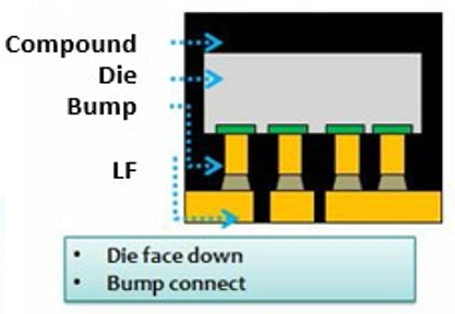
FCQFN, also known as Flip Chip Quad Flat No lead Package, is an advanced packaging technology developed on the basis of QFN packaging.
Product Features
Superior electrical performance
Efficient signal transmission: The inverted chip structure shortens the electrical connection path between the chip and the package, reduces signal transmission delay, has good high-frequency characteristics, reduces signal reflection and crosstalk, and is suitable for fields such as 5G communication and high-speed data transmission that require high signal processing speed and stability.
Low resistance and low inductance: Pin free design and internal structure optimization have reduced pin inductance and resistance, resulting in low self inductance coefficient and wiring resistance inside the package. This can effectively reduce energy loss during signal transmission and improve circuit efficiency.
Good heat dissipation performance
Large area heat dissipation channel: The large exposed heat pad at the bottom can be directly soldered to the system PCB, providing a good heat dissipation channel for the chip, which can quickly dissipate the heat generated by the chip and avoid the chip’s performance degradation or damage due to overheating.
Low thermal resistance: Compared with traditional packaging, FCQFN packaging has significantly lower thermal resistance, which can effectively reduce chip operating temperature, improve chip reliability and service life, and meet the heat dissipation needs of high-power devices.
Compact packaging size
Small footprint: The pinless design and compact structure make the FCQFN package small in size and occupy less PCB board area, which is conducive to achieving miniaturization and lightweight of electronic devices. It has obvious advantages in products such as smartphones and wearable devices that require strict space requirements.
Lightweight: Overall lightweight, in line with the trend of modern electronic device lightweight development, has a positive impact on the battery life and portability of portable electronic devices.
application
Mobile phones, tablets, laptops, etc., used for power management chips, wireless communication chips, audio chips, etc
process characteristics
High precision requirements for flip chip mounting
Adopting flip chip technology requires high-precision equipment and processes to ensure the accuracy and consistency of chip flip chip mounting. Strict process control is required in processes such as bump fabrication, chip alignment, and soldering to ensure electrical connection and mechanical stability between the chip and the packaging substrate. For example, precise control of the height, shape, and position of the bumps, as well as the alignment accuracy between the chip and the substrate, is usually required to achieve micrometer level or even higher precision.